Glow Discharge Optical Emission Spectroscopy (GD-OES)
Few techniques are capable of directly detecting and measuring hydrogen in materials. GD-OES provides a means to measuring the composition and concentration of any element, including hydrogen, at depths up to 10-100's of µm with nanometer depth resolution.
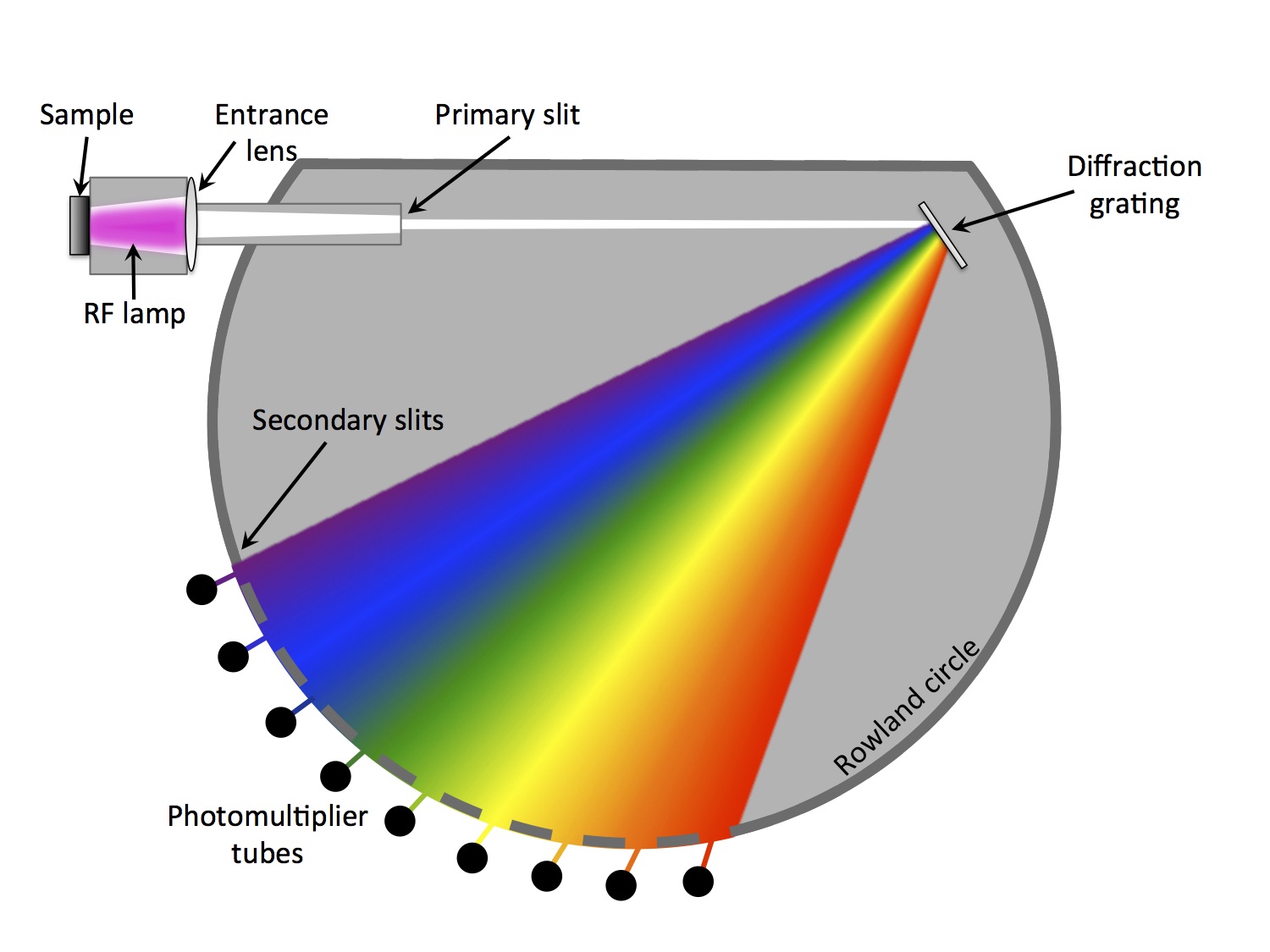
A radio frequency plasma is used to etch a 2-10 mm diameter crater in a conductive or non-conductive sample. The eroded material is optically stimulated from the plasma and the light from the plasma is transmitted into the analyzer section. The analyzer section separates the light through a diffraction grating into its different wavelengths, where each wavelength corresponds to a different element. An array of photomultiplier tubes simultaneously measure the elements of interest. The system also contains a monochromator, which is capable of analyzing almost any additional wavelength that may not have a dedicated photomultiplier tube. An integrated
interferometry system measures the real-time depth of the eroded crater.
The GD-OES located at STAR is configured for 10's of elements ranging from hydrogen, to iron, to tungsten.
|  |
Principle of glow discharge optical emission spectroscopy (GD-OES)
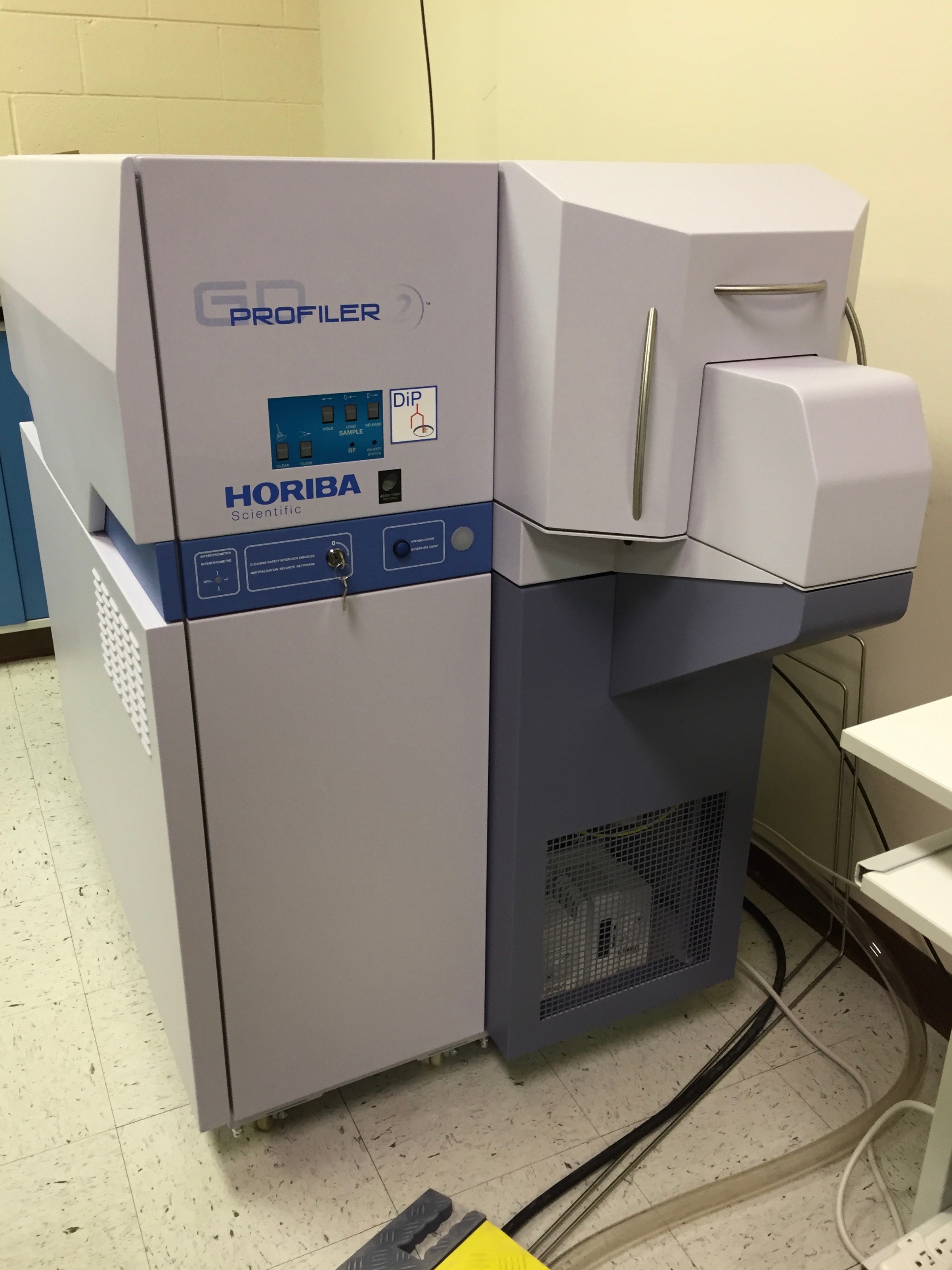
| GD-OES located in STAR laboratory
|
Contact: Chase Taylor | (208) 533-4068 | Email Contact
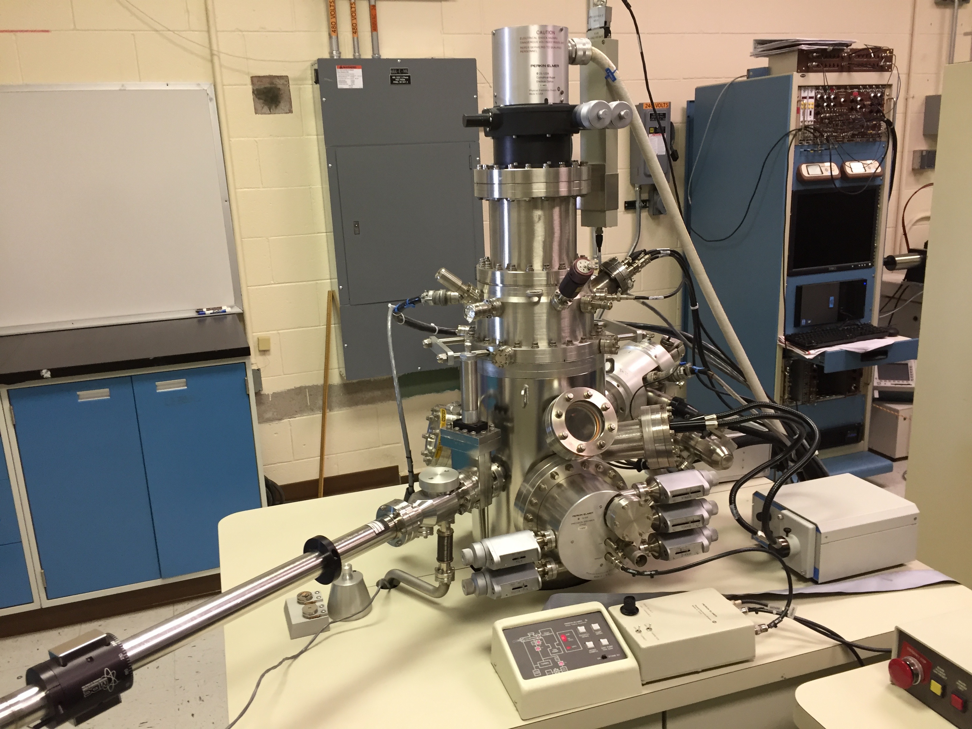
X-ray Photoelectron Spectroscopy (XPS)
Surfaces dictate how materials interface and interact with their environment. This is especially true for phenomena such as permeation and plasma-surface interactions. XPS is used to measure the surface chemistry of materials that occurs within depths of 1-10 nm.
Low energy X-rays are generated as a high voltage filament releases electrons that impact an Al or Mg anode, selected for either higher resolution or intensity, respectively. The X-rays interact with the sample being interrogated and, through the photoelectric effect, release electrons. The kinetic energy of these photoelectrons is detected in a hemispherical analyzer. The binding energy, which is used to identify the chemical composition of the sample, is easily calculated as the difference between the incident X-ray energy and the photoelectron kinetic energy and work function.
The PHI 5600-LS XPS system at the STAR laboratory is configured with a dual anode X-ray source, a high-resolution monochromatic X-ray source, an ion beam sputter gun for depth profiling, and an electron flood gun for charge neutralization. The large sample platen allows for dozens of samples to be mounted simultaneously, which can be programmatically analyzed.
|
Contact: Chase Taylor | (208) 533-4068 | Email Contact
Scanning Auger Microprobe (SAM)
Equipped with a rastering LaB6 filament-generated electron beam, a cylindrical mirror analyzer, and a secondary electron detector, this versatile diagnostic is capable of performing Auger electron spectroscopy (AES) as well as scanning electron microscopy (SEM).
AES provides the surface elemental composition of samples. Because the electron beam can raster, this enables elemental mapping of the surface (<5 nm). SAM elemental mapping differs from conventional mapping systems (e.g., energy-dispersive X-ray spectroscopy, EDS) found in typical SEMs, which provide information from the bulk material (1-3 µm).
SEM produces high magnification images of sample surfaces. Many processes modify the micro- and nano-structure of materials. Under fusion relevant divertor conditions, the Tritium Plasma Experiment at STAR can cause micro-fuzz to grow from tungsten surfaces. Plasma and ion irradiation can cause blistering of metals. These phenomena and more can be characterized using the SAM.
|
Scanning Auger microprobe (SAM) at the STAR laboratory
|
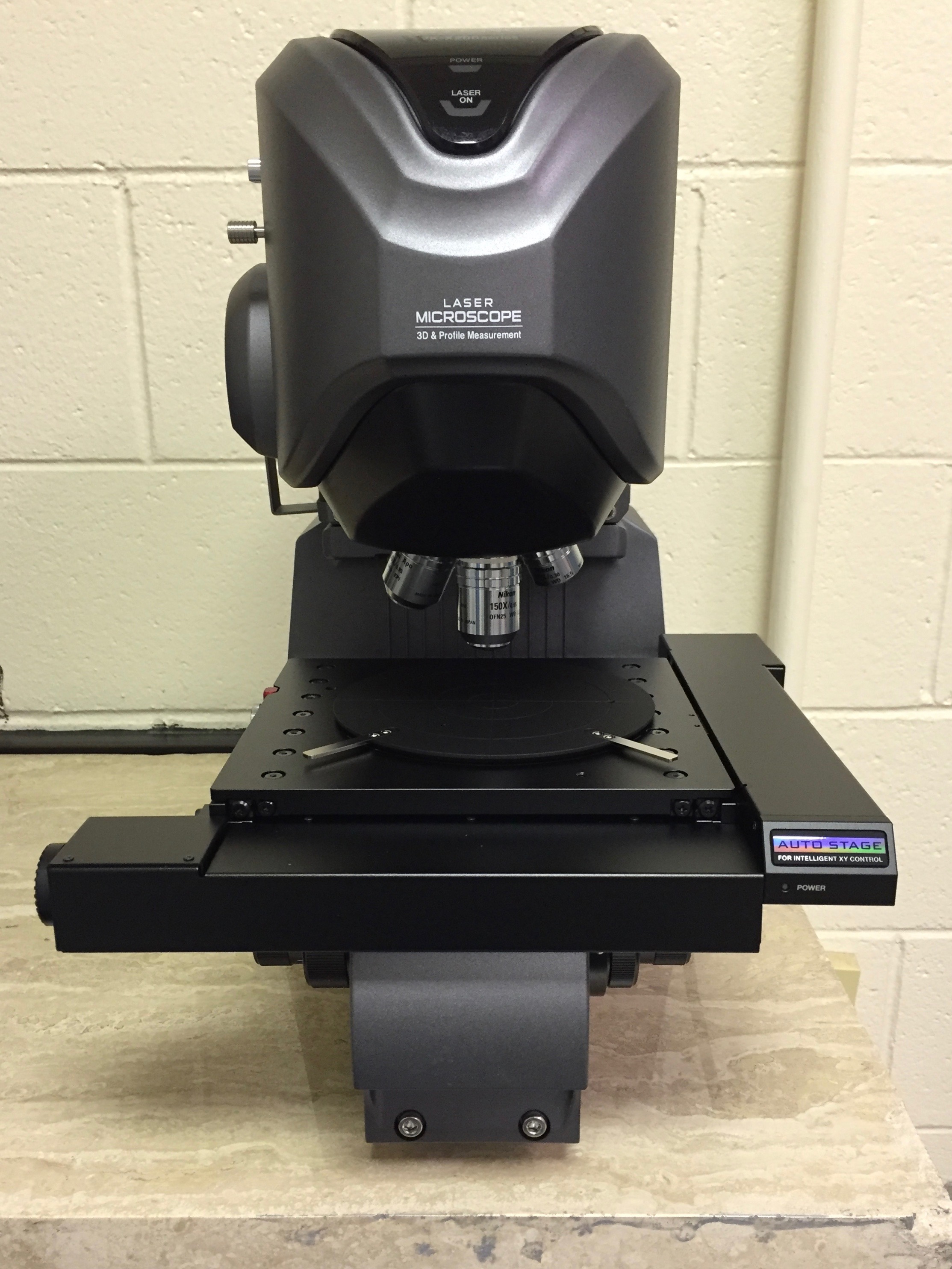
Confocal Laser Scanning Microscope (CLSM)
A 3D laser scanning confocal microscope can be use for quick, atmospheric, sub-micron sample imaging, where virtually no sample preparation is required. The microscope combines standard optical microscopy with a scanning laser to produce high resolution 3D images. Height data is obtained as the laser light is reflected from the sample to a photomultiplier tube (PMT). A small pinhole aperture is located in front of the PMT and allows only light that is completely in focus to be detected. By changing the objective lens height to bring the laser light in focus, and repeating this for every X-Y position on the sample, the height data can be applied to the standard optical image for full 3D reconstruction. The CLSM also offers non-contact profilometry, ASTM grain size measurements, particle counting, and a host of other measurements.
|
Confocal laser scanning microscope (CLSM) at the STAR laboratory
|
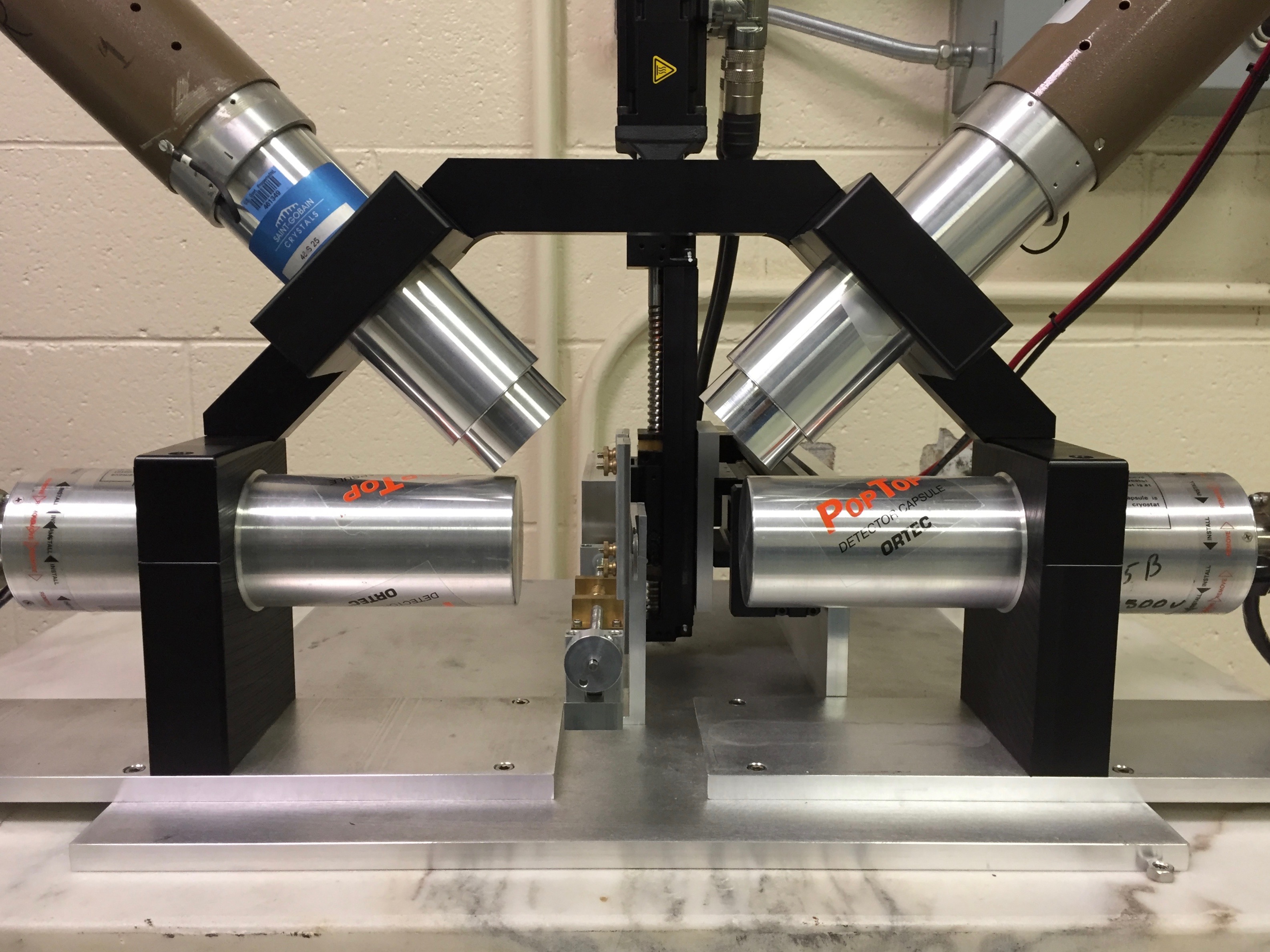
Positron Annihilation Spectroscopy (PAS)
At the atomic scale, all materials have defects in the form of occasionally missing atoms. High powered transmission electron microscopes are capable of measuring large clusters of these missing atoms, however, PAS is the only technique that is sensitive to a single missing atom.
PAS utilizes positrons, or anti-electrons, that are emitted from a radioactive source, typically 22Na. Positrons from the source enter an adjacent sample and almost immediately slow down and begin a random walk through the atomic crystal lattice. If the positively charged positrons encounter a vacancy where an atom, or a cluster of atoms, is missing, the positron becomes trapped by the repulsive positive charge of the atoms lining the vacancy. Eventually, the positron will collide with an electron. When any antimatter touches its matter-counterpart, the pair annihilates -- in this case the mass of the positron and electron undergo a pure conversion into energy. This energy is detected as two 511 keV photons, which are emitted almost exactly 180º from each other.
At the STAR laboratory, two PAS systems are used to measure defects in materials.
Coincidence Doppler broadening (CDB) PAS uses two high-purity germanium detectors to measure the subtle shift in energy in the 511 keV annihilation photons. Positrons that annihilate with electrons at vacancies (valence electrons) produce annihilation photons close to 511 keV, while annihilation events with electrons in the defect-free bulk tend to deviate farther from 511 keV. This small difference provides a relative measure of defect concentration from one sample to another.
Positron annihilation lifetime spectroscopy (PALS) employs two ultra-fast scintillating detectors. At almost exactly the same moment a positron is emitted from 22Na, another photon is also released. One of the fast detectors measures this 1274 keV photon, marks it as a start signal, and starts a timer. The stop signal is registered when the other detector measures the 511 keV annihilation photon. The time difference between the start and stop signal (i.e., positron lifetime) is a mere few hundred picoseconds (0.0000000001 sec). The lifetime is directly proportional to the size of the defects.
PAS measurements are important for understanding the mechanical properties of materials, catalysis efficiency, radiation induced defects, semiconductor quality, among many other applications. For fusion materials, deuterium and radioactive tritium fuel become trapped in vacancies. PAS is especially important in correlating vacancy concentration and size to the amount of trapped deuterium and tritium.
|
Positron annihilation spectroscopy (PAS) at the STAR laboratory
|
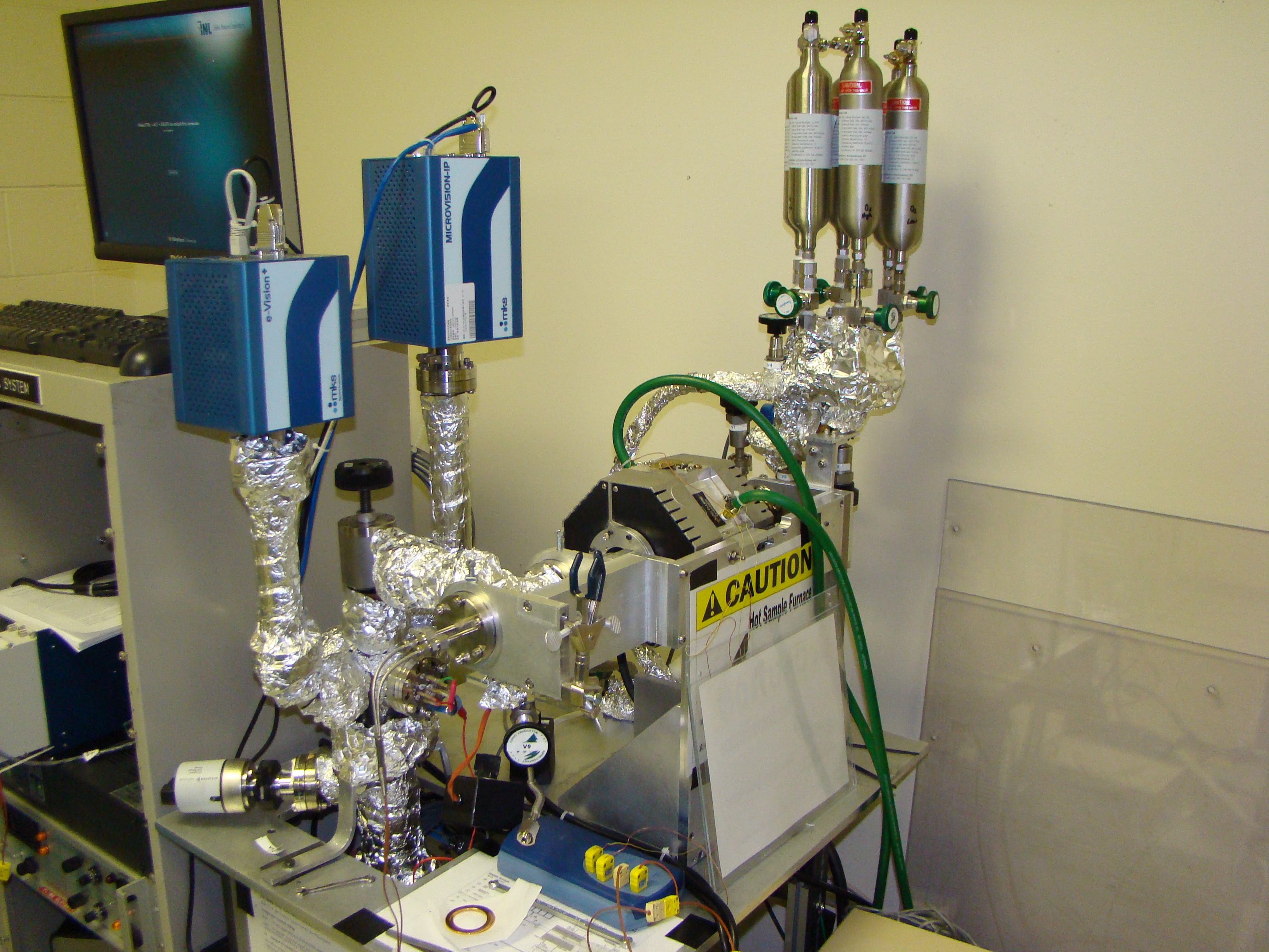
Thermal Desorption Spectroscopy (TDS)
Fusion relevant gases, such as deuterium, tritium, and helium, become implanted in plasma-facing materials in fusion reactors. Because fusion reactors will have a regulatory limit of how much tritium they can have on site, it is important to understand and limit how much tritium is stuck in plasma-facing surfaces.
The total amount of deuterium, tritium, or helium that is trapped in materials can be investigated and determined using TDS. To do so, a sample is heated at a very controlled rate. Quadrupole mass spectrometers are used to measure the gases that come out of the sample. Correlating the gas emission with temperature helps determine the microstructural trapping mechanism in the material.
The TDS system at the STAR laboratory uses an infrared tube furnace (Tmax = 1100ºC), and directly measures the sample surface temperature using redundant thermocouples. Of the two mass spectrometers on the system, a high resolution unit is used to measure the minute mass difference between D2 and He (both nominally 4 amu). The system is calibrated using several NIST traceable leak rates for each gas of interest.
|
Thermal desorption spectroscopy (TDS) system at the STAR laboratory
|
General Information
Each of the diagnostics at the STAR laboratory have been designed or customized to allow for the analysis of tritium contaminated or low activation radioactive samples. However, non-destructive analysis, and interchangeable parts for destructive analysis, avoids cross-contamination of clean samples.